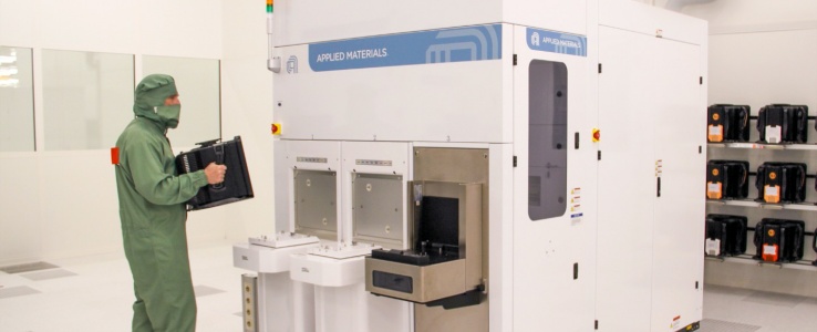
Applied Materials to create 'Europe´s largest tech hub'
Applied Materials will team up with 300mm semiconductor research centre Fraunhofer Institute for Photonic Microsystems to open a new technology hub for semiconductor metrology and process analysis.
Source: evertiq.com